If the history of DRAM1 were a thriller, every increase in capacity would be stalked by that monster of complexity, speed. At MHz speeds, DRAM was sufficiently slow that it could be characterised by a couple of numbers -- the access time being the most important. Now, though, it's fast enough that physical limits, such as the speed of light, are an important part of the design process. At the speeds that DRAM operates nowadays, the wires representing the connection between DRAM and its controller (part of the CPU die) behave less like an instantaneous transport of signal and more like a series of crowded parallel shipping lanes, where individual bits move leisurely to their destination, some arriving sooner than others, interfering with their neighbors, and bouncing off the dock.2 If you don't have a handle on the dynamic behaviour of signal transmission to and from the RAM, you simply won't be able to communicate with it.
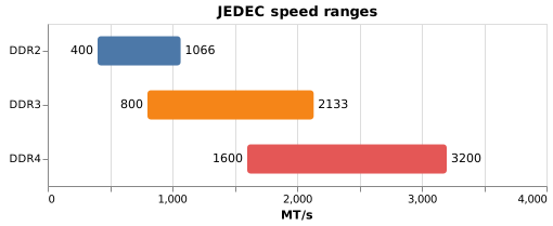
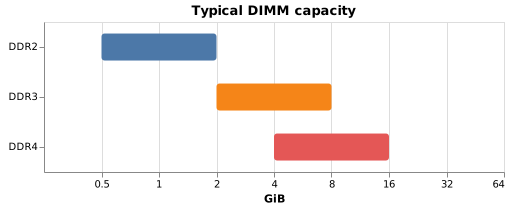
RAM training is about discovering dynamic timing and voltage numbers
In other words, you can't think about DRAM by itself any more. To talk to it, you need to take into account the static and dynamic characteristics of the system comprising DRAM, controller, and system board. This is the general domain of RAM training -- discovering the timings, resistances, and, in some cases, voltages which allow for the most efficient communication between system and RAM, while also of course retaining accuracy.
If you've got a sufficiently gamer-focused PC you might have ventured into the RAM configuration settings, showing any of: extreme memory profile, which is a terrifying name for something relatively dull; various timings like "CAS latency", "RAS", "tRTP"; voltage adjustments, and so on. These aren't the sort of things that RAM training discovers: these are old-school static parameters, and they exist because the RAM you buy is typically faster than the specification it meets.3 You can look these up on manufacturer sites and forums. The dynamic parameters can't, by definition, be determined ahead of time. Instead, RAM training runs at least every time the device starts up, and adjustments to speed and voltage may be made continuously throughout the runtime of the system.
Training axes
Fundamentally, training does one thing: for a given tunable parameter -- or axis -- of timing or voltage, determine the maximum and minimum workable values, and choose the middle one -- the voltage or timing which is equidistant from both extremes. The trick is doing this for all axes. Each generation of RAM (DDR, DDR2, DDR3, LPDDR, etc up until the now-current DDR5) adds more axes but typically doesn't remove any. We're going to look at three specific generational examples of the hardware before looking at how this works in code.
The three generations we'll look at in detail are LPDDR2, DDR3, and DDR4. The following table summarises the major training axes used by these generations.
| Name | Purpose | LPDDR2 | DDR3 | DDR4 |
|---|---|---|---|---|
| Driver impedance (ZQ) | Impedance-match DDR and controller pins to bus | ✓ | ✓ | ✓ |
| ODT calibration | Manage signal reflection for multiple RAM cards | ✗ | ✓ | ✓ |
| Write levelling | Matches clock signal to data signals | ✗ | ✓ | ✓ |
| DQS training | Matches DQS to data signals for reading | ✗ | ✓ | ✓ |
| Read / write VREF centering | Determine appropriate "middle" voltage for distinguishing 0 and 1 | ✗ | ✗ | ✓ |
As you can see, axes tend to accumulate. Also:
- The DRAM side gets more complex. Earlier DDR specifications put almost all the onus on the controller; later ones require the RAM also to be parameterisable. This gets interesting in the next post, when we look at the software side.
- Axes aren't just about timing but also about power output, power input (threshold voltages to distinguish ones from zeroes), and impedance (see below).
- "Dynamic" doesn't just mean "at boot time". Even earlier specifications require or support periodic re-parameterisation at runtime to compensate for voltage and temperature changes.
A short digression into impedance
When you put a signal onto a line, care must be taken to ensure that the impedance of the driver and line match (for more information on impedance, see the sidebar). If the impedances don't match, the signal is partially reflected. This is bad for digital signals as the reflected wavefront could interfere with the next signal on the wire.
To stop this, signal drivers must impedance match to the transmission line. They do this by effectively adjusting their resistance on a per-pin basis. The way this works is quite interesting: the driver for each line has multiple legs, each of which can be enabled or disabled. Because each leg is effectively an extra connection to the same pin, and conductances of parallel paths add, the more enabled legs, the lower the resistance. Impedance matching on a line is thus enabling the appropriate number of legs such that the resistance of the driver matches the characteristic impedance of the line. Since the supply voltage is always the same, and the resistance is the sum of the driver's impedance and the line's characteristic impedance, by Ohm's law impedance matching (which changes the impedance of the driver) effectively changes the amount of current used by the driver to put a signal onto the line6.
LPDDR2 (2009)
LPDDR2's simplicity comes from its lack of flexibility and low speeds. It was designed to be non-removable and in particular was intended for embedded devices such as phones (LP stands for Low Power). This means there's less dynamic variation to worry about (no capacitance or extra length introduced by a socket) and the traces can be much smaller -- millimetres or less.
Here's a photo of the original Raspberry Pi (click to enlarge):
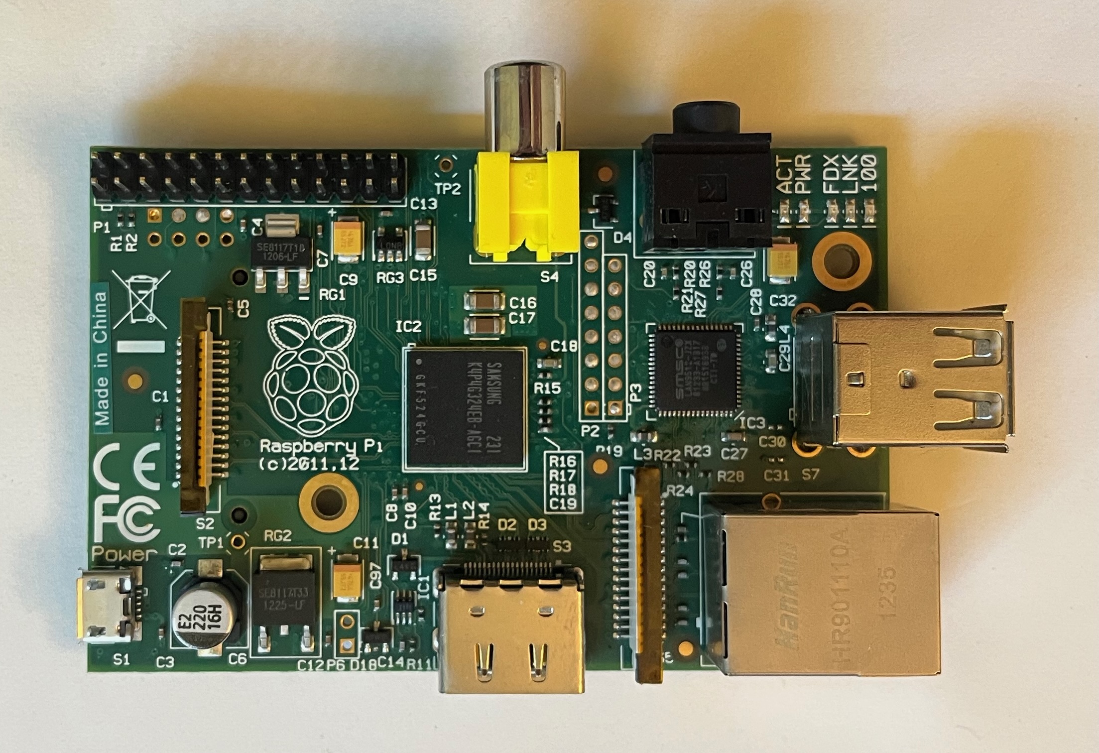
The CPU is in the centre. Given that Raspberry Pis use Broadcom chips, you might be surprised by the Samsung markings. This is because the Broadcom BCM2835 which implements both ARM CPU and VideoCore GPU is underneath, and BGA-soldered directly to, the Samsung DRAM4. This package-on-package design minimises the number of variables which might introduce voltage or timing variances when communicating with the RAM.
Consequently, LPDDR2's dynamic requirements aren't that complex. Both sides simply perform impedance calibration. The (LP)DDR family of specifications calls this type of impedance matching ZQ calibration, following the standard letter for impedance (Z) and JEDEC's convention for pins used as outputs (Q). LPDDR has a specific pin called ZQ which is connected to a high-precision resistor of known value (240Ω) which acts as ground truth. During RAM initialisation, the controller outputs a ZQINIT command to the DDR, which causes it to calibrate its output drivers using the ZQ pin as a reference. The DDR will also periodically recalibrate during operation. This is sometimes also called PVT calibration, because it compensates for variations in Process (manufacturing variations), Voltage, and Temperature.
ZQ calibration is symmetric: the DDR controller also performs its own form of ZQ calibration for its output drivers using the same mechanism (of a dedicated high-precision resistor).
Interestingly, LPDDR2 doesn't bother with the receiving end of the equation. This means that signals sent by the DDR or the controller do indeed "bounce off" the receiver's pins and reflect back along the wire. However, the lines are so short, and the speed of the RAM so (relatively) low, that by the time the signal has stabilised the reflection has already happened (and been absorbed by the impedance-matched driving side). The JEDEC name for this is High-Speed Unterminated Logic (HSUL) -- a slightly-misleading name. The lines are also only pulled low or high by the driver -- if neither controller nor DRAM is driving, the bus floats. Again, this is only something you can get away with in short point-to-point connections.
And that's it for LPDDR2. Its tiny transmission lines, and relatively low speed, mean that this transmit-only impedance matching is all that's required for reliable performance. But it's not always possible to solder RAM directly to an SoC or put it right next to its controller on a mainboard. Sometimes it needs to live further away on the mainboard, or even (gasp) be removable7. This is the domain of the non-low-power DDR family, such as DDR3.
DDR3 (2007)
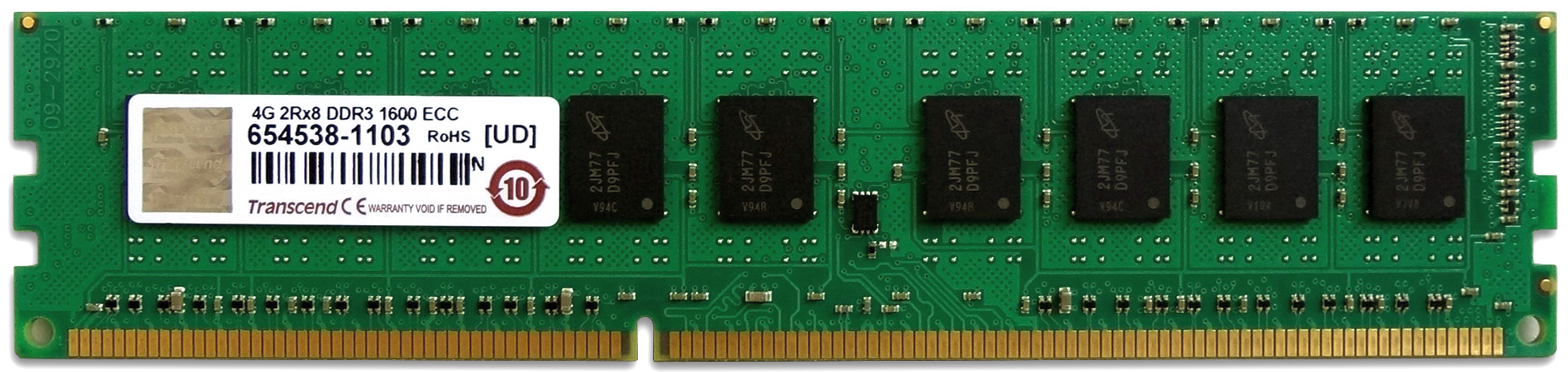
DDR3 is designed to support flexibility of placement. It may be soldered to a different part of the main board, or it may be socketed, like this module for PCs:
Support for increased speeds, a variety of connectivity options, and significantly longer buses makes DDR3 a much more complicated system, electrically, than LPDDR2. The additional training steps over LPDDR2 reflect this:
- DDR3 is faster, which means more potential for interference from reflected signals, so the specification adds bus termination at the DRAM side.5
- Traces are longer, and some are point-to-point while others use a bus topology. Speeds are now fast enough that these can arrive at different times, which must be taken into account.
- For similar reasons training happens on a per-bit basis for the data lines.
The DDR3 bus uses a different termination strategy called SSTL. Resistors pull the bus to VDDQ/2 when it's at rest, and it moves between 0 and VDDQ (1.5V) when driven. This ensures that signals do not reflect, but it also consumes power even when idle.
ZQ calibration
Like LPDDR2, DDR3 performs impedance matching in the form of ZQ calibration. Unlike LPDDR2's output-only impedance matching, DDR3 also does impedance matching for the receive side by using the ZQ calibration to adjust On-Die Termination (ODT). The key driver for this is that while LPDDR2 is a point-to-point protocol, DDR3 is a bus where multiple RAM modules can connect:
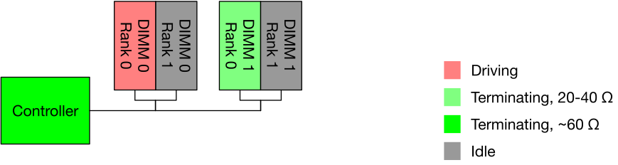
In the diagram, DIMM 0, rank 0, is driving. Data placed on the DQ bus will travel in both directions, towards the controller and towards DIMM 1. In order to ensure the signal does not reflect at the DIMM 1 end, DIMM 1 enables ODT on one of its ranks -- but not both, as the ranks are sufficiently close together that they are effectively one point on the bus.
If more DIMMs are added, each additional non-selected DIMM performs termination. However, the individual ODT is higher, because two DIMMs are terminating in parallel, halving the effective resistance.
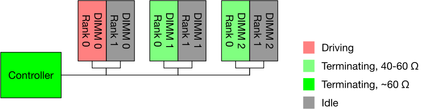
The termination applied by the controller may also vary with number of DIMMs, as adding DIMMs changes bus capacitance, and adding additional terminations can reduce effective voltage, since only a small number of fixed termination values can be chosen.
Write levelling
Each DRAM module has multiple chips on it, but only one clock signal input. This means that the DRAM chip closest to the socket will receive CK first, then the next chip will receive it a little later, and so on. However, each chip gets its own DQS signal -- "data strobe", which signals to the RAM when data is ready for it to receive on the bus. That means it's very likely that the interval between CK and DQS will be different at each chip.
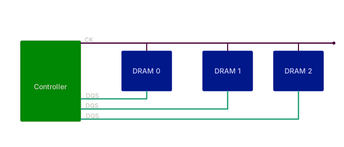
Write levelling addresses this: the controller puts each DRAM chip into a special mode where it listens for DQS and toggles a data pin. The controller can then assert DQS after some delay; if the data pin is not set, then DQS arrived before CK and the controller should increase the delay.
Read and write timing centering
Both reads and writes make use of the data bus DQ and the data strobe DQS. For reads, the DRAM sets DQ and DQS at the same time, and the centering operation is about reading DQ in the middle of the valid window. For writes, the controller aims to ensure that DQS is strobed in the middle of the valid DQ window from the DRAM's perspective. The reason for this asymmetry is to keep the DRAM simple: all the timing work happens in the controller.
The first aspect of read centering is calculating per-line deskew, to ensure that all bits are received at the same time. Each DQ line on the controller side has a programmable delay. To align the DQ lines, the controller adjusts the delay on each line individually until all bits are changing at the same time.
Once the DQ lines are deskewed, the controller can train DQS for reading. It does this in a similar way: it slowly moves its DQS delay and notes the leading and trailing edges of the DQ transition. In other words, if the DRAM is sending 1 on DQ0, with no DQS the controller may not yet read a 1 as the signal is not yet stable. But with a DQS delay that is too high, the DRAM may already have switched DQ0 to the next bit. The controller then stores a DQS delay that is halfway between the leading and trailing edges.
For write training, it's the controller's job to ensure the DRAM sees DQS strobe in the middle of the viable period for the data. This builds neatly upon read training -- the controller adjusts parameters while writing to RAM, and then reads back the values that it's written to verify that they were written correctly. It's the same two steps as for read centering.
- DQ deskew: The controller does this by writing data to the DRAM while varying the DQ write delay on a per-line basis, then reading back the value to find the leading and trailing edges.
- DQS centering: With deskewed DQ, write a pattern to DRAM, read it back while adjusting DQS delay. The middle valid value is stored.
DDR4 (2012)
Surprise, DDR4 is faster. It also changes the way the bus is powered and terminated.
Most obviously, it drops the operating voltage to 1.2V (from DDR3's 1.5V). This by itself is a win for speed: voltage levels move at a fixed rate, so less of a level shift means edges stabilise faster.
But DDR4 goes further than this by also changing the bus termination strategy (again!) to Pseudo-Open Drain (POD12). In POD, the bus rests at 1.2V, which means the controller or DDR drivers only ever need to pull it low.8 And in DDR4 (and later), the drivers don't actually pull down to 0V, but instead some fraction of VDDQ -- even smaller voltage swing, even faster speeds.
But now the transition voltage isn't known, and it changes with board parameters and things like drive strength and temperature. DDR4 data lines must now be trained along both voltage and time axes.
Glossary
| Name | Definition |
|---|---|
| DQ | Data lines |
| DQS | Data strobe -- signals transmission of data |
| MT/s | RAM speed -- megatransfers per second (multiply by 8 to get MB/sec) |
| ODT | On-Die Termination: impedance-matching for transmission lines |
References
-
DRAM, or Dynamic RAM, is the type of RAM that pretty much everything uses if it needs it in the order of gigabytes (or higher). It's cheaper than its traditional opposite, Static RAM, but requires special handling to ensure that it doesn't lose its stored values while running. We don't need to know too much more than this for this story. This is the first and last time this article will gloss over a technical detail about RAM, so please savour it. ↩
-
I'm informed that the analogy breaks down here, at least until I patent my design for a ship with giant springs mounted at both ends. ↩
-
Specifically, DDR5, say, has to meet or exceed the timing requirements specified by JEDEC for DDR5, but a) it can report its actual sometimes-significantly-better maximum safe operating parameters to the BIOS, which is the Extreme Memory Profile (XMP) thing, and b) you may want to do things like increase the voltage, if the RAM can handle it, to trade power and heat efficiency for performance. ↩
-
Package-on-package is very convenient but somewhat limiting; Raspberry Pi 3 retained the LPDDR but switched to soldering the package to the underside of the board -- directly underneath the CPU. This made it easier to offer multiple variants of the Pi 3 with differing amounts of RAM. ↩
-
This is not a DDR3 innovation (it's in DDR2), but LPDDR2 does not include it. ↩
-
Why are we only taking the driver's impedance and the line's characteristic impedance into account, and not thinking about the impedance of the receiver? Because we're talking about the dynamic behaviour of the system. Signals take time to propagate, so at the time of actually putting a signal onto the line, the only parts which count is the driver and the thing directly connected to it. The impedance of the receiver only matters when the wave actually gets there (because this is where reflections happen if the receiver is not impedance-matched). ↩
-
Removable without a heat gun, that is. Everything is removable if you're brave enough. ↩
-
This combines nicely with another DDR4 feature, Data Bus Inversion, which biases the bus towards high logic levels. ↩